
Description
CD4049 – Hex Inverting Buffer/Converter IC
The CD4049 hex buffers are monolithic complementary MOS (CMOS) integrated circuits constructed with N- and P-channel enhancement mode transistors. These devices feature logic-level conversion using only one supply voltage (VDD).
The input signal level can exceed the VDD supply voltage when these devices are used for logic-level conversions. These devices are intended for use as hex buffers, CMOS to DTL/TTL converters, or as CMOS current drivers, and at VDD=5.0V, they can drive directly two DTL/TTL loads over the full operating temperature range.
check out :
Pinout:
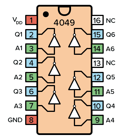
Pinout Of CD4049 IC
| Pin Name | Pin # | Type | Description |
|---|---|---|---|
| VDD | 1 | Power | Supply Voltage (+3 to +15V) |
| GND | 8 | Power | Ground (0V) |
| Q1-Q6 | 2, 4, 6, 10, 12, 15 | Input | Inputs to the inverters |
| A1-A6 | 3, 5, 7, 9, 11, 14 | Output | Outputs from the inverters |
| NC | 13, 16 | | Not Connected |
Applications:
- CMOS hex inverter/buffer
- CMOS to DTL/TTL hex converter
- CMOS current “sink” or “source” driver
- CMOS high-to-low logic level converter
Package Includes:
Selected qty of IC – CD4049
Specifications:
| Part number | CD4049 |
| Technology Family | CD4000 |
| VCC (Min) (V) | 3 |
| VCC (Max) (V) | 18 |
| Channels (#) | 6 |
| Output type | Push-Pull |
| Input Type | Standard CMOS |
| ICC @ nom voltage (Max)(mA) | 600 |
| Features | Standard speed (tpd > 50ns), Over-voltage tolerant inputs, Unbuffered |
| IOL (Max) (mA) | 18 |
| IOH (Max) (mA) | -3.1 |
| Rating | See Data Sheet |
| Data rate (Mbps) | 24 |
| Package Group | PDIP|16 |


Reviews
There are no reviews yet.